- +64 9 269 6916
- +64 9 269 6926
Learn about printed circuit board and stencil technology and empower your business!
PCB Technology
Glossary and Abbreviations - PCB Glossary
Click on an alphabet below to directly jump to the chosen alphabet section...
ABCDEFGHIJKLMNOPQRSTUVWXYZAlphabet S
- SchematicA diagram which shows, by means of graphic symbols, the electrical connections and functions of a specific circuit arrangement.
- ScoringA technique in which grooves are machined on opposite sides of a panel to a depth that permits individual boards to be separated from the panel after component assembly.
- Screen PrintingA process for transferring an image from a patterned screen to a substrate through a paste forced by a squeegee of a screen printer.
- Short: Short circuitAn abnormal connection of relatively low resistance between two points of a circuit. The result is excess (often damaging) current between these points. Such a connection is considered to have occurred in a printed wiring CAD database or artwork anytime conductors from different nets either touch or come closer than the minimum spacing allowed for the design rules being used.
- Short runDepends on the size of the manufacturing facility and the size of the printed circuit boards to be made. A short manufacturing run of printed circuits means from one to tens of panels of pcbs required to fulfill the order rather than hundreds.
- Silk Screen (Silk Legend)Epoxy-ink Legend printed on PCB. The most common colors used are white and yellow.
- Sieber MeyerIn order to process your order, we require a drill file (with x:y coordinates) that is viewable in any text editor
- Single Side PCBThe pads and traces are on the one side of the board only.
- Single trackPCB design with only one route between adjacent DIP pins.
- Small Outline Integrated Circuit (SOIC)An integrated circuit with two parallel rows of pins in surface mount package.
- Size X & YAll dimensions are in inches or metric. If board is in metric, please convert to inches. Please note, maximum X & Y configuration 108" This means if the width (X) is 14", then the maximum length (Y) is 7.71".
- SMOBCSolder mask over bare copper.
- SMDSurface Mount Device.
- SMTSurface Mount Technology.
- Solder BridgingSolder connecting, in most cases, misconnecting, two or more adjacent pads that come into contact to form a conductive path.
- Solder BumpsRound solder balls bonded to the pads of components used in face-down bonding techniques.
- Solder CoatA layer of solder that is applied directly from a molten solder bath to a conductive pattern.
- Solder LevelingThe process by which the board is exposed to hot oil or hot air to remove excess solder from holes and lands.
- Solder Mask or Solder resistCoating to prevent solder to deposit on.
- Solder MaskUsed to protect the board and circuitry during the assembly and packaging operations. Among other things, the solder mask helps prevents solder bridges between adjacent pads and traces during the wave soldering process.
- Solder Mask (Artwork)To generate your Soldermask artwork, add your smallest space measurement to the pad size. For boards with 0.006" spaces, use a pad size up to +0.006" up to 0.010" for 0.010". Spaces larger than 0.010" should have a pad size of +0.010".
- Please noteWhile we make every attempt to leave a mask "dam" between surface mounts, fine pitch areas will be relieved in strips. Our manufacturing process needs at least 0.005" mask "dam" between pads in order to adhere to the board. Pad-to-pad spacing less than 0.013" may not have solder mask between them.
- SolderMaskColorThere are different types of colour used for solder mask, for e,g Green, Red, Blue and white etc..
- Solder pasteAssociated with SMT. A paste screened onto a pcb or panel of pcbs to facilitate the placing and soldering of surface mount components. Also used to refer to the Gerber file used to produce the stencil/screen.
- Solder WickA band of wire removes molten solder away from a solder joining or a solder bridge or just for desoldering.
- SPCStatistical Process Control. The collection of process data and creation of control charting is a tool used to monitor processes and to assure that they remain in control or stable. Control charts help distinguish process variation due to assignable causes from those due to unassignable causes.
- Step-and-RepeatThe successive exposure of a single image on order to produce a multiple-image production master. Also used in CNC programs.
- StuffComponents are attached and soldered to a printed circuit board. Often done by an assembly house.
- Sub-PanelA group of printed circuits arrayed in a panel and handled by both the board house and the assembly house as though it were a single printed wiring board. The sub-panel is usually prepared at the board house by routing most of the material separating individual modules leaving small tabs.
- SubstrateA material on whose surface adhesive substance is spread for bonding or coating. Also, any material that provides a supporting surface for other materials used to support printed circuit patterns.
- Surface MountThe pitch of the surface mount is defined as the dimension in inches from center to center of surface mount pads. Standard pitch is >0.025", fine pitch is 0.011"-0.025", and ultra fine pitch is < 0.011". As boards contain finer pitch, processing and test fixture costs increase.
- Surface finishIt is the type of finish required by customer for his board. The different surface finishing processes are HASL, OSP, Immersion gold, Immersion silver, Gold plating for all of regular boards.
PCB Design Tips
When designing a PCB, try to limit the amount of draws you use. Draws use a lot of memory and slow the programming time. Use a flash for pads instead.
More tips...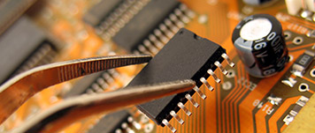
Contract Assembly
We are one-stop solution provider for all your contract assembly requirements. We have the capability and resources to provide PCB assemblies, as well as cable and harness assemblies.


What our customers say?
QualiEco Circuits Limited is an excellent supplier to us! We appreciate the quality of service and support that we receive from QualiEco Circuits. They always deliver what is promised
For printed circuit boards (PCBs) or PCB assembly you can count on. Talk to the friendly and experienced team at QualiEco Circuits, New Zealand.