- +64 9 269 6916
Learn about printed circuit board and stencil technology and empower your business!
PCB Technology
Glossary and Abbreviations - PCB Glossary
Click on an alphabet below to directly jump to the chosen alphabet section...
ABCDEFGHIJKLMNOPQRSTUVWXYZAlphabet P
- PadThe portion of the conductive pattern on printed circuits designated for the mounting or attachment of components.
- Pad annulusTypically refers to the width of the ring of metal around a hole in a pad.
- Part NumberThe name or number associated with your printed circuit board for your convenience.
- PanelA rectangular sheet of base material or metal-clad material of predetermined size that is used for the processing of printed boards and, when required, one or more test coupons.
- PatternThe configuration of conductive and nonconductive materials on a panel or printed board. Also, the circuit configuration on related tools, drawing, and masters.
- Pattern PlatingThe selective plating of a conductive pattern.
- PCBPrinted Circuit Board. Also called Printed Wiring Board (PWB).
- PCB databaseAll of the data fundamental to a PCB design , stored as one or more files on a computer.
- PCB-Design-Software/ToolsSoftware that helps designer to do schematic, layout design, routing and optimizations, etc. There are many design software and tools in the market. Some of them are free PCB design software. Here is a short list: ExpressPCB, EAGLE, PROTEL, CADSTAR, ORCAD, CIRCUIT MAKER, P-CAD 2000, PCB ELEGANCE, EDWIN, VISUALPC, BPECS32, AUTOENGINEER, EXPERT PCB, CIRCAD, LAYOUT, CIRCUIT LAYOUT, MCCAD, DREAM CAD, E-CAD, POWERPCB, PCB ASSISTANT, PCB DESIGNER, QCAD, QUICK ROUTE, TARGET 3001, WIN CIRCUIT 98, BOARD EDITOR, PCB, VUTRAX, CIRCUIT CREATOR, PADSPCB, DESIGN WORKS, OSMOND PPC, LAY01, SCORE, GElectronic, PRO-Board, PRO-Net , CSIEDA, VISUALPCB, WINBOARD, ULTIBOARD, EASY PC, RANGER, PROTEUS, EPD - Electronics Packaging Designer , AutoTrax Eda, Sprint Layout, CADINT, KICAD, Merlin PCB Designer, FREE-PCB, TinyCAD, WINQCAD, Pulsonix, DIPTRACE.
- PCB Fabrication ProcessA general process can be simplified as: Copper laminate -> Drill board -> Deposit Cu -> Photolithography -> Tin lead plate or finishing -> Etch -> Hot air level -> Solder mask -> E-Testing - > Routing/V-scoring -> Product inspection -> Final cleanning -> Packaging . (Note : Procedure is same for manufacturing but varies with respect to different manufacturer)
- PCMCIAPersonal Computer Memory Card International Association.
- PECPrinted Electronic Component.
- Phenolic PCBIt is cheaper laminate material different from fibre glass material.
- Photographic ImageAn image in a photo mask or in an emulsion that is on a film or plate.
- Photo PrintThe process of forming a circuit pattern image by hardening a photosensitive polymeric material by passing light through a photographic film.
- Photo-PlottingA photographic process whereby an image is generated by a controlled light beam that directly exposes a light-sensitive material.
- Photo-ResistA material that is sensitive to portions of the light spectrum and that, when properly exposed can mask portions of a base metal with a high degree of integrity.
- Photo-toolA transparent film that contains the circuit pattern, which is represented by a series of lines of dots at a high resolution.
- PinA terminal on a component, whether SMT or through-hole. Also called a lead.
- PitchThe center-to-center spacing between conductors, such as pads and pins, on a PCB.
- Pick-and-PlaceA manufacturing operation of assembly process in which components are selected and placed onto specific locations according to the assembly file of the circuit.
- PTHPlated Through Hole, a hole with the plated copper on its sides to provide electrical connections between conductive patterns at the levels of a printed circuit board. There are two types of PTH. One is for mounting components and the other is not used to mount component.
- PlatingThe chemical or electrochemical process in which metal is deposited on a surface.
- Plating VoidThe area of absence of a specific metal from a specific cross-sectional area.
- Plastic Leaded Chip Carrier (PLCC)A component package with J-leads.
- Plating ResistMaterial deposited as a covering film on an area to prevent plating on this area.
- PlotsThe masters for photo-tools produced from Gerber files.
- PositiveDeveloped images of photo-plotted file, where the areas selectively exposed by the photo-plotter appear black and unexposed areas are clear. For outer-layers, color will indicate copper. Positive inner-layers will have clear areas to indicate copper.
- PrepregA sheet of material that has been impregnated with a resin cured to an intermediate stage. I.e. B-stage resin.
- PlatenA flat plate of metal within the lamination press in between in which stacks are placed during pressing.
- PrototypeA pcb made and built to test a design.
PCB Design Tips
When designing a PCB, try to limit the amount of draws you use. Draws use a lot of memory and slow the programming time. Use a flash for pads instead.
More tips...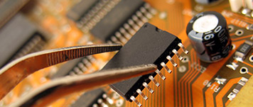
Contract Assembly
We are one-stop solution provider for all your contract assembly requirements. We have the capability and resources to provide PCB assemblies, as well as cable and harness assemblies.


What our customers say?
QualiEco Circuits Limited is an excellent supplier to us! We appreciate the quality of service and support that we receive from QualiEco Circuits. They always deliver what is promised
For printed circuit boards (PCBs) or PCB assembly you can count on. Talk to the friendly and experienced team at QualiEco Circuits, New Zealand.